
AESEMI invites you to our next webinar, organized in collaboration with ZEISS, which will take place on Tuesday, March 10, at 4:00 p.m. We will address a topic of great relevance to the sector: “Advances in Microscopy for the Semiconductor Industry: Solutions from ZEISS.”
Currently, the semiconductor industry faces increasingly complex challenges that require innovative and precise solutions. Advanced microscopy has become an essential tool for research, development, and quality control in this field.
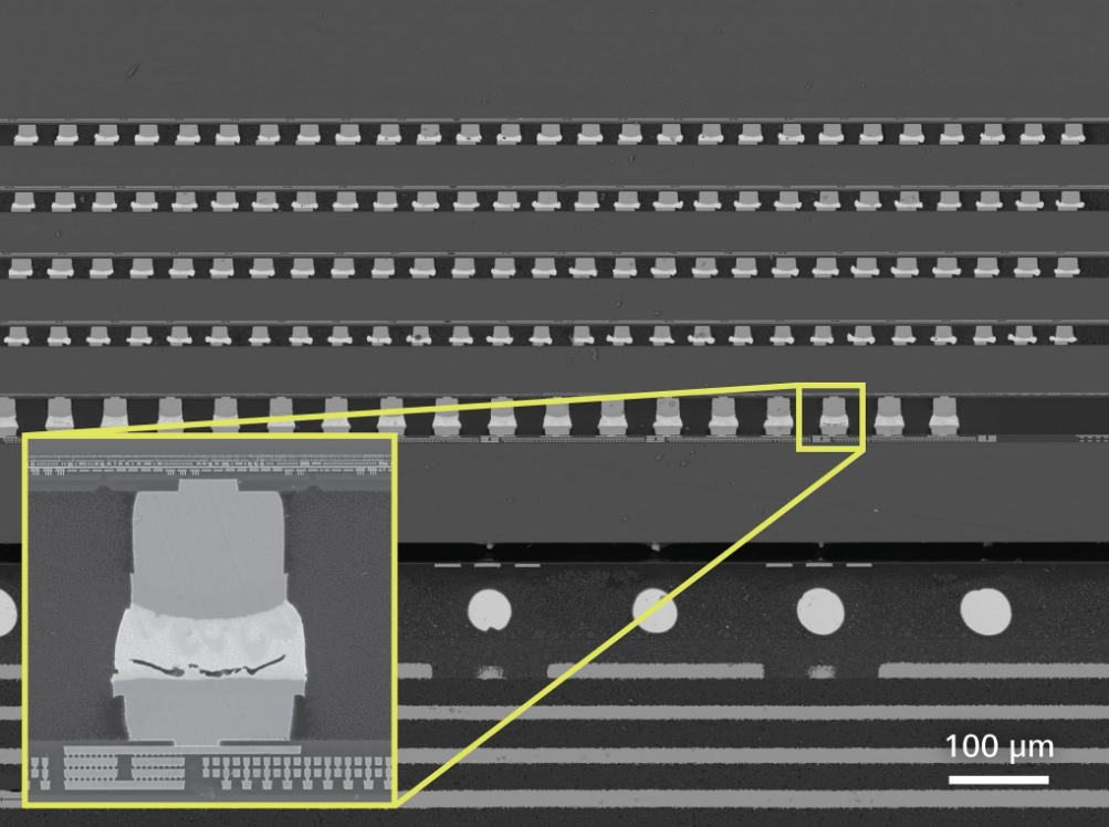
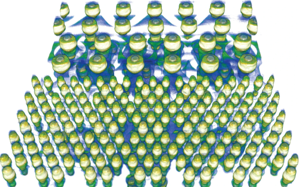
During this session, we will learn about ZEISS’s electron microscopy and X-ray solutions, widely used in metrology, quality control, and research applications in the semiconductor industry, as well as their complementarity with production-oriented systems. The webinar will allow attendees to discover the available technological capabilities and their impact in highly demanding industrial environments.
We encourage you to participate in this session, which will offer a practical overview of key technologies for driving innovation and competitiveness in the sector.
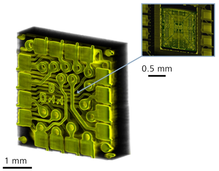
X-ray microtomography of a gyroscope obtained in less than 1 minute.
Date: Tuesday, March 10, 2026
Time: 4:00 p.m. – 5:00 p.m. (CET)
Location: Online