
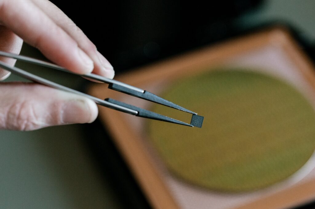
Summary. The digital economy is built on trust, and that trust begins with the invisible foundations of infrastructure: entropy. At Quside, we develop Level 4 quantum random number generators (QRNGs), the standard that not only produces random bits, but also measures, verifies and monitors them in real time. This vision of global trusted infrastructure is realised in a very concrete way: choosing the Indium Phosphide (InP) platform and standard manufacturing processes to integrate photonic circuits at the chip level, validating each die in wafer-level testing (WLT), and using commercial Quad Flat No-Lead (QFN) packaging that allows for scalable production with stability and repeatability.
Digital trust infrastructure, built on good entropy
Every transaction, key, or session depends on a common ingredient: strong randomness. If entropy fails, the entire system inherits that failure. That is why we talk about four levels of maturity in randomness generation: from illusion (Level 1) to quantified and verified uncertainty (Level 4). The latter is what really supports critical infrastructures such as HSM, KMS, data centres or post-quantum deployments.
The four levels of randomness, from illusion to measured control
– Level 1, illusion. Fixed or repeated values. Guaranteed disaster.
– Level 2, opportunistic. Human or system inputs, useful only as a supplement.
– Level 3, designed chaos. TRNG with ring oscillators, avalanche diodes or QRNG, strong but with blind spots if only validated with statistics.
– Level 4, quantified uncertainty. Dedicated physical sources with explicit entropy modelling, real-time estimation, and continuous verification. This is the gold standard for highly demanding environments.
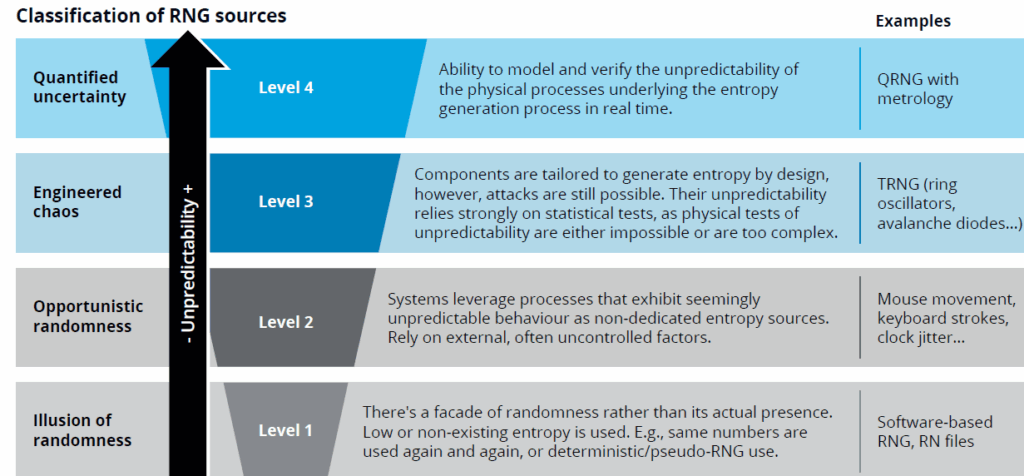
At Quside, we position ourselves at Level 4 because we do not assume entropy; we measure it, model it, and audit it. And we do so from the physical base, on the chip itself.
The technological choice: InP for integrated photonics
Our QRNG technology is based on the phase diffusion process in semiconductor lasers, a genuinely unpredictable optical phenomenon. To integrate it at scale, we have opted for the indium phosphide (InP) platform:
– Native integration of lasers and detectors. The InP ecosystem allows high-speed lasers and photodetectors to be combined on the same photonic integrated circuit, reducing complexity and packaging costs.
– Speed and signal-to-noise ratio. The InP platform supports high-frequency operation, allowing us to achieve entropy generation rates in the Gbit/s range with low latency and excellent signal-to-noise ratio.
Process maturity and stability. The use of standardised processes in InP allows for better control over manufacturing variations, facilitating high levels of reproducibility and reliability. In this context, the chip acts as a physical source of analogue entropy. This signal must then be digitised and processed by a cryptographic extractor, accompanied by continuous health monitoring tests as described in the NIST SP800-90 standard. In this way, the system not only generates random bits, but also provides real-time evidence of the quality of the entropy generated.
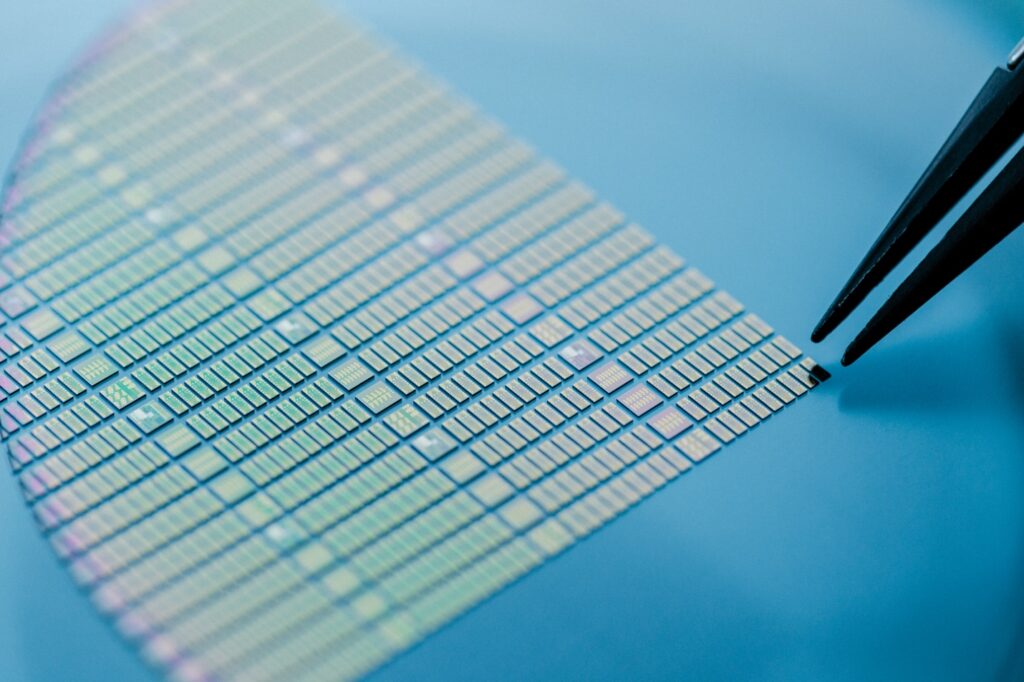
Validation from the wafer: Entropy-oriented WLT
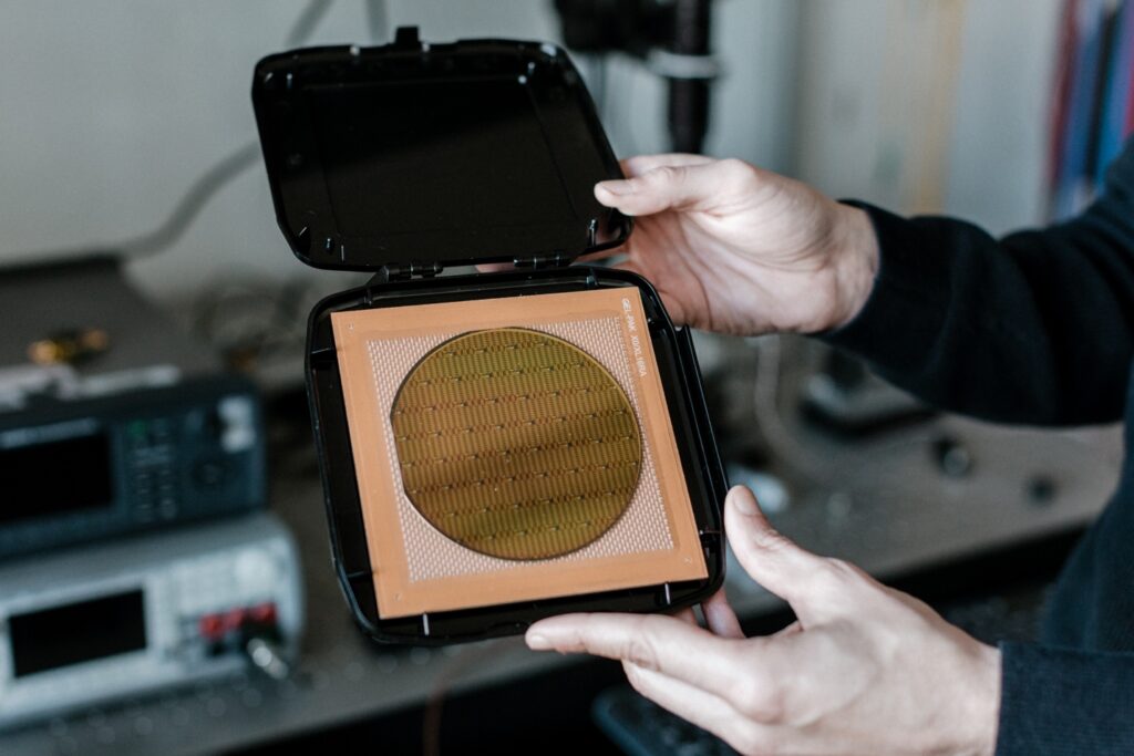
An essential step on the path to Level 4 is the validation of chips at the wafer level, Wafer-Level Testing (WLT). At this stage, we ensure that the manufacturing process has been carried out correctly. Through specific tests, we identify and discard chips with electrical or photonic faults, ensuring that only functional devices advance to the next stages, meeting the signal quality and stability requirements that will later enable them to achieve reliable entropy. The validation of their behaviour as an entropy source is carried out later, once they have been encapsulated and integrated into a dedicated test module.
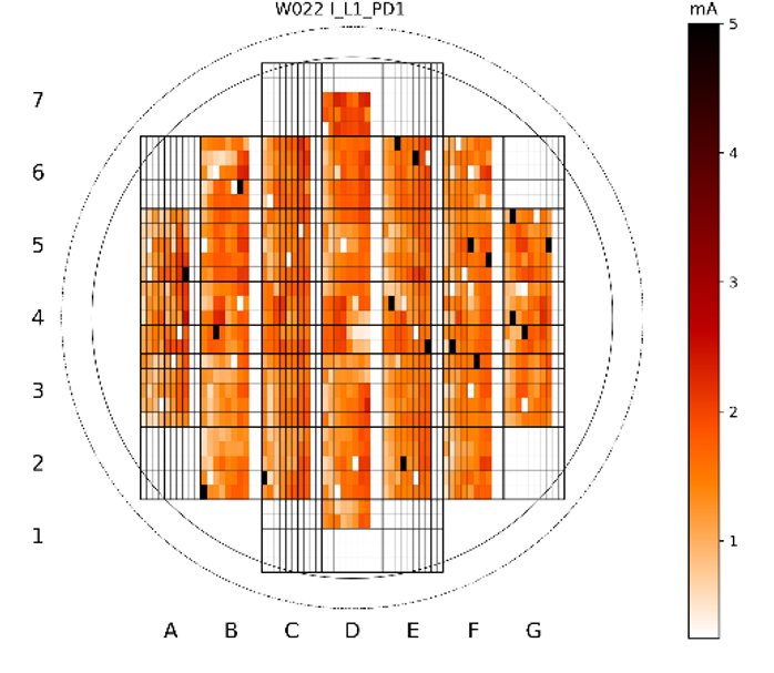
At this stage, we use an automated analysis process that generates a map of functional chips on each wafer, clearly differentiating between those that are ready for integration and those that are out of range. This approach allows us to guarantee that, right from the start of the production chain, only those devices capable of offering the expected level of security move forward.
With this methodology, quality is not only validated at the end of the cycle, but is ensured from the outset, providing consistency in performance, scalability in manufacturing, and complete traceability from the wafer to the final system.
Scalability: QFN packaging for volume and stability
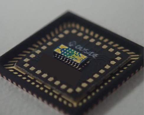
To bring these laboratory QRNGs to mass deployment, packaging is critical. We have chosen to encapsulate our chips in QFN format, a standard widely used in microelectronics. Although it is a photonic device, its design does not require optical fibres, allowing conventional electronic packaging processes to be used.
The use of QFN offers us key advantages:
– Optimised thermal management, thanks to the exposed pad that stabilises the chip’s operating point.
– Low electrical parasitics, essential for maintaining signal quality in high-speed applications.
– Industrial scalability in terms of costs and volume, as this format is fully compatible with high-production SMT lines.
In this way, the photonic chip packaged in QFN becomes a reliable and reproducible physical source of quantum noise. Conversion into a complete QRNG is achieved in subsequent modules, where readout electronics, digitisation, cryptographic extractors and entropy validation functions are added, in accordance with international standards such as NIST SP800-90B.
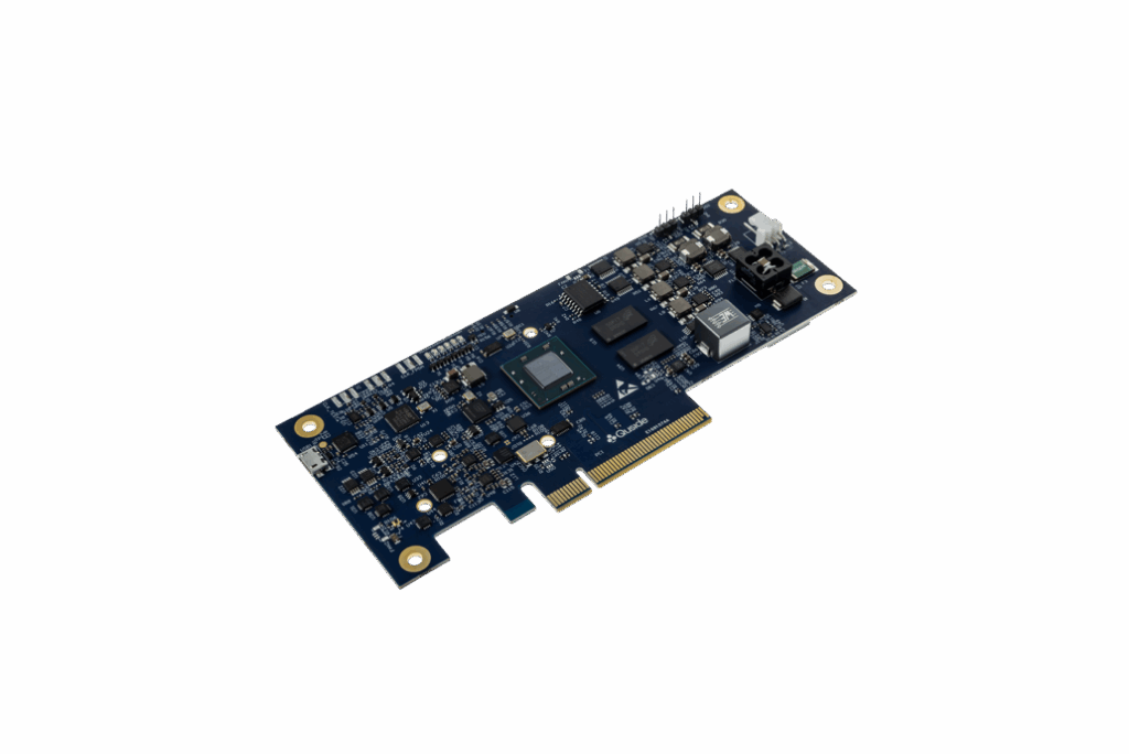
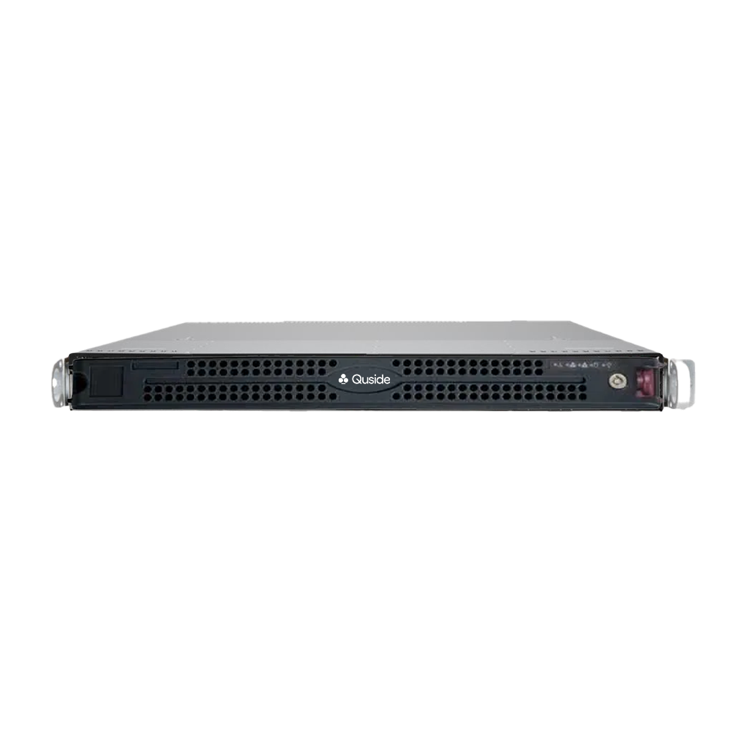
From wafer to data centre: how everything connects
The result of this process is a family of QRNG modules operating at Gbit/s speeds, with integrated telemetry and auditable entropy evidence. Entropy sources in photonic chips power everything from PCIe cards for data centres to modules that can be integrated into HSMs and cloud platforms, becoming the foundation of the new digital trust infrastructure.
Conclusion
The trusted infrastructure of the future is not built on assumptions, it is built on evidence. Committing to InP, integrating metrology into the chip, validating on the wafer with WLT and packaging in QFN has allowed us to scale Level 4 QRNGs from the laboratory to industrial production. At Quside, we believe that this groundwork in semiconductors is what will enable digital trust to remain possible both in the present and in the post-quantum era.
Domenico Tulli (Cofundador y CTO) y Ferran Bardaji (COO)