

Idoia Haro Alonso
Vaifro Dariol
Gabriel Caffarena Fernández
An example of strategic capacity-building in microelectronics, telecommunications and artificial intelligence.
Malaga Microelectronics Centre: capabilities for the networks of the future
Europe’s digital transformation requires in-house capabilities in strategic areas such as telecommunications, artificial intelligence and semiconductors. Against this backdrop, the Malaga Microelectronics Centre project, launched in 2022, has enabled Vodafone Intelligent Solutions to strengthen its capabilities in research, development and validation of technologies for future mobile networks.
This project has been funded under the Recovery, Transformation and Resilience Plan, through the C12.I4 – PERTE Chip investment, approved by the Spanish Government and coordinated by the Ministry of Industry and Tourism. It is also aligned with the Important Project of Common European Interest on Microelectronics and Communication Technologies, IPCEI ME/TC.
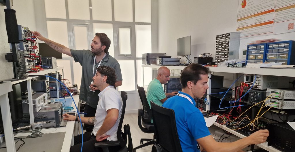
Not only have ASIC solutions been developed, but an end-to-end Open RAN (Radio Access Network) laboratory with chip design, prototyping and testing capabilities has also been set up at the Vodafone Innovation Hub in Málaga. This environment enables a holistic approach to the process, ranging from algorithms and processing architectures to their implementation and validation on telecommunications platforms. The combination of network, software and silicon capabilities makes it easier to study technologies not as isolated elements, but as parts of a complete system.
Activities carried out
Throughout the project, work has been carried out on the integration and testing of Open RAN systems, ASIC design and verification, integrated photonics applied to the radio unit, the evaluation of computing platforms and energy optimisation, as well as the use of AI for RAN optimisation. All of this combines expertise in networking, algorithms, software and silicon. In this publication, we have selected three examples to illustrate the scope of the capabilities developed.
Integrated photonics for next-generation radio units
In collaboration with the University of Málaga, Vodafone has explored the transfer of beamforming functions to the optical domain using integrated photonics. Beamforming is a technique that coordinates signals from multiple antenna elements to concentrate transmission or reception in a specific direction, thereby improving coverage and capacity. This line of research addresses a fundamental requirement for next-generation radio units: to process and direct signals from multiple antenna elements whilst keeping complexity, signal loss and power consumption under control.
The work has progressed from the conceptual stage to initial validation, including the development of Vodafone’s first photonic chip for optical beamforming and its evaluation in configurations comprising 16 antenna elements. This progress has enabled the functional definition to be linked to the device design and to the analysis of its integration into a communications architecture. Consequently, the research has not been limited to the photonic component alone, but has also considered its contribution within the radio system.
In-house simulation tools have also been developed to study beam steering, beam squint (the deviation in beam direction as the frequency changes), insertion losses and performance prior to manufacture. These tools make it possible to predict the behaviour of different configurations and analyse how decisions made in the optical domain affect the overall result. The ability to simulate, compare and validate in advance bridges the gap between a technological idea and its evaluation in a representative configuration.
Taken together, this work paves the way for more efficient, accurate and scalable radio units.
Intel 18A-P technology and hardware acceleration for Massive MIMO
The Málaga Microelectronics Centre is also strengthening its strategic partnership with Intel Foundry to work with Intel 18A-P, the most advanced semiconductor manufacturing technology. Access to and learning about these types of processes enable the development of high-performance, low-power silicon blocks for AI-RAN and for future 5G and 6G networks, whilst strengthening the ability to design proprietary solutions within the chip ecosystem.
Building on this technological foundation, Vodafone is developing its own MU-MIMO equalisation IP for the uplink, aimed at next-generation radio systems. The solution is designed for integration into both radio unit (RU) baseband processors and base station (DU) acceleration platforms. As a reusable hardware block, it can facilitate its incorporation into future semiconductor designs and reduce the effort required to develop new platforms.
The work has included the definition of the architecture, RTL development and ASIC verification, with particular attention paid to scalability, high performance and the adaptation of power consumption to network demand. This line of work demonstrates how knowledge of communications algorithms can be translated into advanced silicon and become reusable, verifiable IP ready for next-generation radio systems.
Benchmarking and efficient computing
The Málaga Microelectronics Centre has also made it possible to consolidate benchmarking capabilities to objectively evaluate processors, accelerators and heterogeneous architectures in the context of the RAN. In an environment where telecommunications and artificial intelligence functions can run on very different platforms, having a common evaluation methodology is essential for comparing alternatives using consistent criteria.
These capabilities enable the analysis of performance metrics such as latency and throughput, as well as energy efficiency, scalability and behaviour under telecommunications and artificial intelligence workloads. The joint evaluation of these parameters prevents decisions from being based solely on peak performance and allows for consideration of the balance between processing capacity, power consumption and adaptability to different levels of demand.
System-level analysis also helps to identify bottlenecks, validate design decisions and verify whether an improvement made to a component actually translates into a measurable advantage under operational conditions. In this way, benchmarking acts as a link between algorithm design, computing platforms and end-to-end validation, providing an objective view of the real impact of processing innovations.
The next stage: from Open RAN to AI-RAN
The capabilities developed at the Málaga Microelectronics Centre provide a solid foundation for the next stage in the evolution of networks: the convergence of telecommunications and artificial intelligence. Vodafone has a strong presence in the AI-RAN Alliance, through which it helps to drive the use of AI to improve the network, integrate intelligence into its functions and leverage shared computing infrastructure for RAN and AI workloads.
The laboratory will evolve by incorporating new computing capabilities for artificial intelligence. This expansion will enable the evaluation of AI-for-RAN workloads (the use of artificial intelligence to optimise RAN performance), the creation of heterogeneous platforms combining in-house developed accelerators and GPUs, and the generation of end-to-end AI workflows covering everything from data ingestion and pre-processing through to training and inference, enabling efficient distribution between the edge and the cloud. The aim is to maintain a comprehensive view of the system and to analyse algorithms, execution platforms, efficiency and network behaviour in conjunction.
De este modo, las soluciones encontradas y el conocimiento acumulado en Open RAN, diseño de chips, aceleración hardware, fotónica, benchmarking, eficiencia energética y despliegue de IA para optimización de la RAN se conectan directamente con AI-RAN. La creación del laboratorio no solo ha generado resultados tecnológicos concretos, sino también una infraestructura y unas capacidades que refuerzan el ecosistema español de semiconductores y preparan el camino hacia redes estandarizadas, inteligentes y eficientes.